UV solution to detect the appearance defects of LED chip packagingReturn >>
2021-01-21 2547
1. Application background
LED (Light-emitting diode) is widely used in the fields of indication and display due to its long life and low energy consumption. The packaging process is one of the main factors affecting the function of the LED. Due to the packaging process itself, there are many defects in the LED packaging process.
2. Application introduction
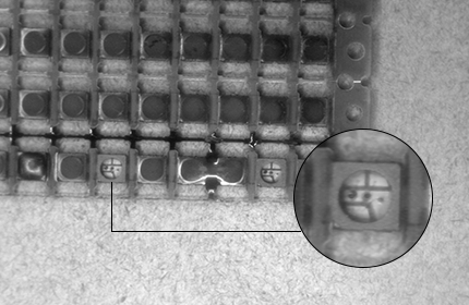
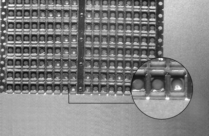
S-UV is a back-illuminated wide-spectrum high-sensitivity sCMOS camera developed by Indigo. The camera's light-sensitivity spans from 180nm to 1100nm, and has a photoelectric conversion efficiency of 60% at 254nm and 50% at 365nm. The appearance of the LED chip package was inspected with S-UV camera under 365nm/254nm ultraviolet light, and the defects of less glue and uneven glue were found.
3. Application advantage
1. Adopting the world's leading scientific-grade back-illuminated sCMOS image sensing technology, 180nm-1100nm ultra-wide spectral response
2. 60%@254nm, 55%@365nm UV enhanced, the shorter the wavelength, the finer the detection
3. Low read noise, full well capacity 100ke, 4MP, 24fps high-speed preview
4. Applications